The Printed Circuit Board
The Printed Circuit Board, or PCB, is a flattened laminated structure consisting of layers of conductive and insulating materials. Embedded in them exist traces and planes of copper material. These have the same functionality as wires but are organized in a way that they occupy less space and do not get knotted and cluttered like wires can. They are easily produced via automated manufacturing systems and are highly consistent because they are made according to universal standards.
A PCB consists of a board that holds components together, provides conductive tracks that connect components, an insulating environment to make sure the electrical current flows via the copper channels as intended, and electrical components that provide the board's desired post-prodction's functionality.
Main Features of PCB's
Components
Components are fastened to the board by soldering them unto conductive pads. They are electrically connected with one another via patterns of copper traces, based on electrical schematics that the drafter has prepared earlier. On double-sided boards interconnections can also be made between the layers on both sides.
Mounting
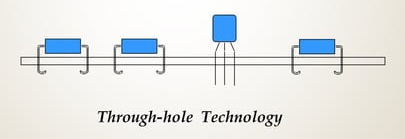
With thisd form of mounting the pins from a through-hole component are instered through small holes and then soldered to hold them in place. The holes lead from the top to the bottom side of the PCB. They are plated with a conductive material (gold or tin)
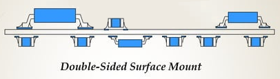
Surface-mounted components are soldered onto surface pads provided by the PCB.
Normally components are placed on the up side of the board but sometimes it is opportune to place components on the opposite site, underneath. You can also add holes, for example, to fasten your board unto a surface. In the latter case the hole does not need to be tinned and you can just use nut/bolt screws.
Tracks / Traces
PCB Components are placed on conductive tracks, aka traces, to form functional electric circuits.
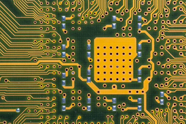
A trace is a copper path along the board through which electrical signals flow which power the attached components. These traces fulfill the same function as electrical wires. albeit more compact and orderly
Masking
Masking refers to the application of a solder mask. This is a protective coating applied to the PCB during manufacturing. It provides:
The mask layer insulates the board to prevent electricity shortcuts between traces or pads.
The mask layer defines the pads and areas for component placement.
The mask layer prevents oxidation on copper traces and pads.
The coating of the mask layer protects against contaminants and corrosion.
The masks have a distinct color to help identify solder and non-solder areas.
Dark green is the most common color of PCB masks. Pads are made by cutting out openings in the mask coating.
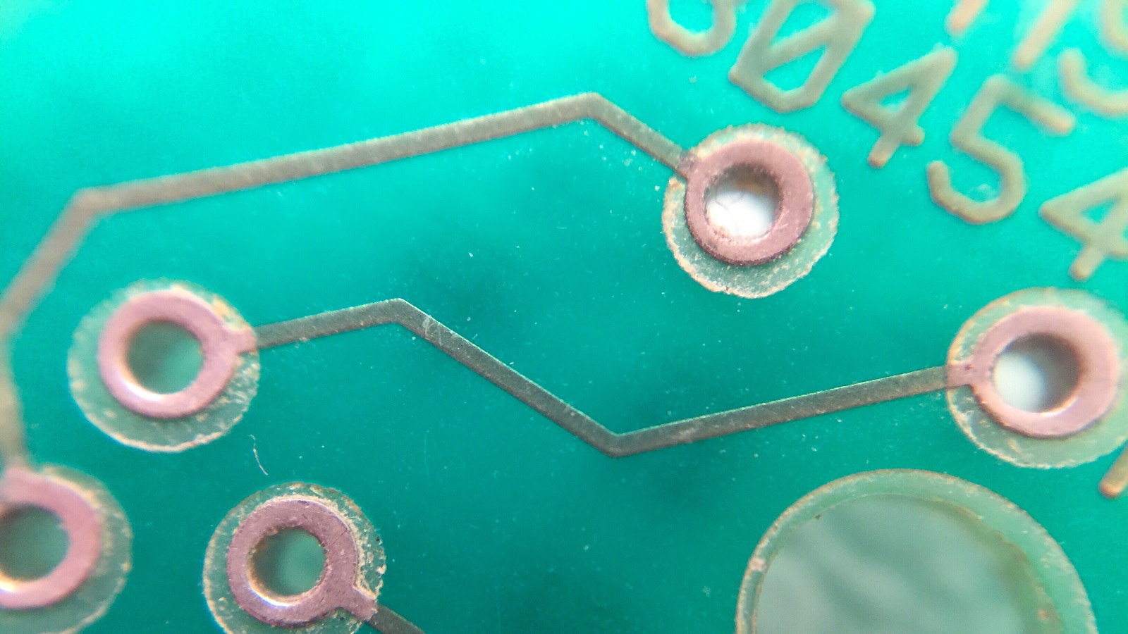
Vias
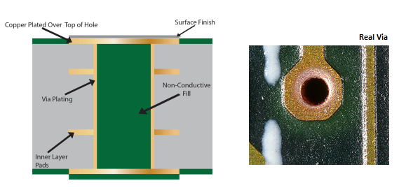
Vias are holes without pad around them. They are not meant for fastening components but for allowing traces to run to other layers within the PCB board. They are lined with copper to trace the power through.
Bridges
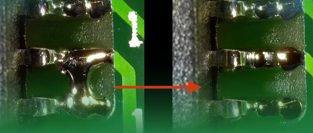
To the left, an accidental solder bridge, to the right the same location after repair.
Bridges are accidental unintended connections formed by leaking solder material. They connect traces or component parts that are not supposed to be conencted.
UNDER CONSTRUCTION